Scientific Notes on Power Electronics: PNP and NPN Transistors
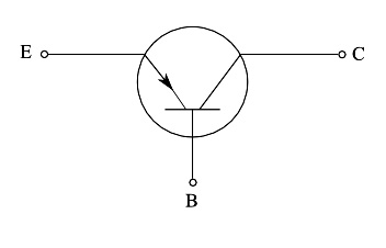
If we try to solder a pn junction to an np junction, we obtain the device shown in Figure 1, where the letters E, B, and C mean Emitter, Base, and Collector, respectively. These are the names assigned to the three regions p, n, p.
We have thus created a PNP transistor.
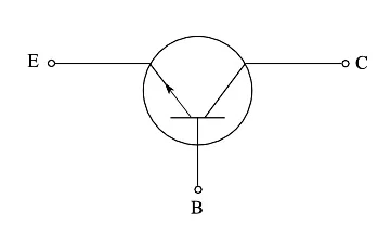
If instead, we solder an np junction to a pn junction, we have the device shown in Figure 2, in which the roles of E, B, and C, concerning doping, are reversed. The result is an NPN transistor. In both configurations, the device consists of junctions JE and JC.
The transistor is also known as a semiconductor triode because it marked the end of the vacuum tube, just as the junction diode replaced the vacuum diode. Another common name is BJT, an acronym for Bipolar Junction Transistor1. The bipolar attribute refers to the electrical conductivity in semiconductors (given by electrons and holes).
In Figure 3 we can see the circuit symbol of the PNP transistor, presented in such a way as to highlight the relationship with the diagram in Figure 1. Similarly, Figure 4 shows the NPN transistor symbol.
Open-circuit transistor
Let’s refer to a PNP transistor (the results immediately generalize to an NPN transistor). In open circuit conditions, we expect behavior similar to that of a single junction, i.e. the presence of a contact potential (see a previous tutorial) which is actually a potential energy barrier whose purpose is that of preventing the diffusion of holes from the emitter to the base. If there were no such barrier, the holes would spread indefinitely towards the base; manifestly non-physical situation as we are in open circuit conditions. If V0 is the height of the barrier at the junction JE, similar arguments will lead us to say that a barrier V′ exists on the junction JC. Assuming the individual regions p,n,p identical with the same concentration of impurities, we have V0 = V′.
The achievement of thermal equilibrium will be characterized by constant values of the concentrations of the minority carriers of the single region:
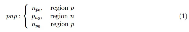
Having used the following convention: the main letter denotes the carrier (electron, hole), and the first subscript indicates the region it belongs to. For example, the symbol np tells us that we are considering electrons in a p region (hence minority charges). Finally, the third subscript 0 indicates that the system is in thermodynamic equilibrium at temperature T0 (which is not necessarily room temperature).
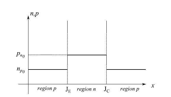
It should be noted that we are neglecting the depletion layer (discussed in a previous tutorial), as it is of negligible size compared to the double junction layer.
In the p-type region, the concentration n is the same because we have assumed these regions to be identical. If in a system of Cartesian axes, we report on the abscissa the linear dimensions of the double junction that constitutes a PNP transistor, and on the ordinate the concentrations of minority carriers in the single region (equation (1)), at the thermodynamic and open circuit equilibrium we will have a trend like that shown in Figure 5, where we assumed pn0 > np0.
It should also be noted that the trends, strictly constant, in the concentrations of minority carriers and in open circuit conditions, are the result of an averaging operation since these quantities fluctuate around an average value, which is the measured one.
Transistor bias
There are more polarization combinations than the diode, thanks to the presence of two junctions and three terminals. As usual, let’s refer to the PNP transistor, directly biasing JE and JC inversely. In Figure 6 we report this polarization configuration, while Figure 7 is the corresponding circuit diagram. Precisely, we have a voltage generator with VEB, while VCC indicates the voltage generated by the battery connected to JC. With VCB we instead indicate the potential difference between collector and base.
Forward biasing of JE reduces the potential barrier (as established in the previous section); this causes diffusion of holes from the emitter to the base and of electrons from the base to the emitter. The result is, therefore, a macroscopic increase in the concentrations of minority carriers in the two regions p and n of JE.
Let’s focus our attention on the widespread holes in the base. Here, we are near JC with the following electric charge configuration: if we measure the potential difference between C and B, we find a value as indicated in Figure 7, and this means that the holes are “collected” by the collector C. However, the JC is inversely biased, and this determines an exponential damping of the holes in the base so that at JC the concentration of these carriers is statistically zero. In turn, the reverse bias of JC causes a reduction in the electron concentration in the p-region of JC, which will dampen exponentially on JC. As stated previously, the concentration of electrons in the p-region of JE undergoes an increase which will then dampen exponentially due to the well-known diffusion mechanism of minority carriers in a junction. These conclusions are summarized in Figure 8.
Source: https://www.slw-ele.com/scientific-notes-on-power-electronics-pnp-and-npn-transistors.html